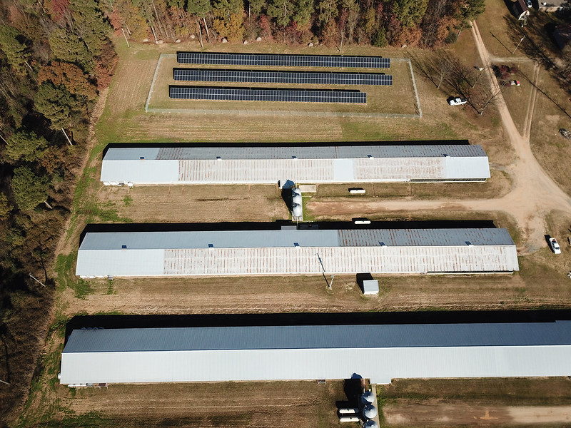
Solar panels: How they work
Contact
University of Arkansas Division of Agriculture
Cooperative Extension Service
2301 S. University Ave.
Little Rock, AR 72204

Solar panels: How they work
I was musing about the solar panel piece I ran two weeks ago when a question occurred to me. Why don’t silicon panels run out of electrons? The original Bell Labs silicon wafers are still working after 75 years, so this must be some kind of perpetual motion machine. I decided to investigate further.
Light has always interested me and I used to spend a fair amount of time discussing different physical aspects of light and explain how these characteristics interacted with plants to accomplish the feat of photosynthesis. This was especially relevant with houseplants where light was oftentimes a limiting factor for growth (and survival). In these interior conditions light could be generated by an array of artificial sources, some of which matched up well with the needs of plants while others less so.
The visible light spectrum is only a small part of the electromagnetic field in which we are continually bathed. The basic unit of this energy spectrum is the photon, a stable particle that has no mass nor electrical charge and travels in a wave form at, well, the speed of light. Explaining the physics behind these wave-packets that Einstein in 1905 called “light quantum” is beyond me, but it is these discreet packets of energy that power solar panels. Twenty years after Einstein’s prediction the name “photon” was adopted when his theoretical work was experimentally proven to be true.
When photons strike a silicon atom they hit an orbiting electron, energizing it and causing it to move to a higher orbit around the silicon nucleus. This displaced electron leaves behind a hole in the orbital plane of the atom, and in the quartz crystal sitting on your shelf, this wayward electron soon looses its energy boost and settles back into the hole left for it. But, the silicon found in solar panels have been specially treated to encourage electron flow, so the hole remains open until a returning electron has dumped its energy load and returned to plug the hole. This process can go on indefinitely with these massless, chargeless photons being the only input into the closed system.
Electrons have a negative charge, so for an electron stream to flow, there must be a positive and negative “terminal” built into the pure silicon chip. The silicon wafer used in photoelectric cells is less than the thickness of a human hair with a positive and negative side that is separated by an interface referred to as the “p-n junction.” One side of the wafer is coated with phosphorus to create the negative “terminal,” and coated with boron on the positive side. Electrons displaced from the negative side of the wafer flow across to the positive side, creating about 0.5 volt differential across the wafer.
The treatment process, called “surface passivation,” was developed in 1954 by Mohamed Atalla, an Egyptian engineer working at Bell Labs. Atalla later worked on the early phases of LED lightbulb development but is best known for his work in computer security and is the “father” of PINs — personal identification numbers.
The current flow created by all of the silicon chips in the panel are directed through a series of “buzz bars” to a microinverter found on each panel that converts the current flow from DC (direct current) to AC (alternating current) power. Alternating current travels a greater distance without power loss so is the type of electricity used in our domestic grid. The energy produced by each panel is fed to an inverter for the entire panel array which adds the energy to the grid.
Check out our resources to see if solar energy is right for your home or business.